1
2
3
4
5
6
7
8
9
10
11
12
Te nanowire device
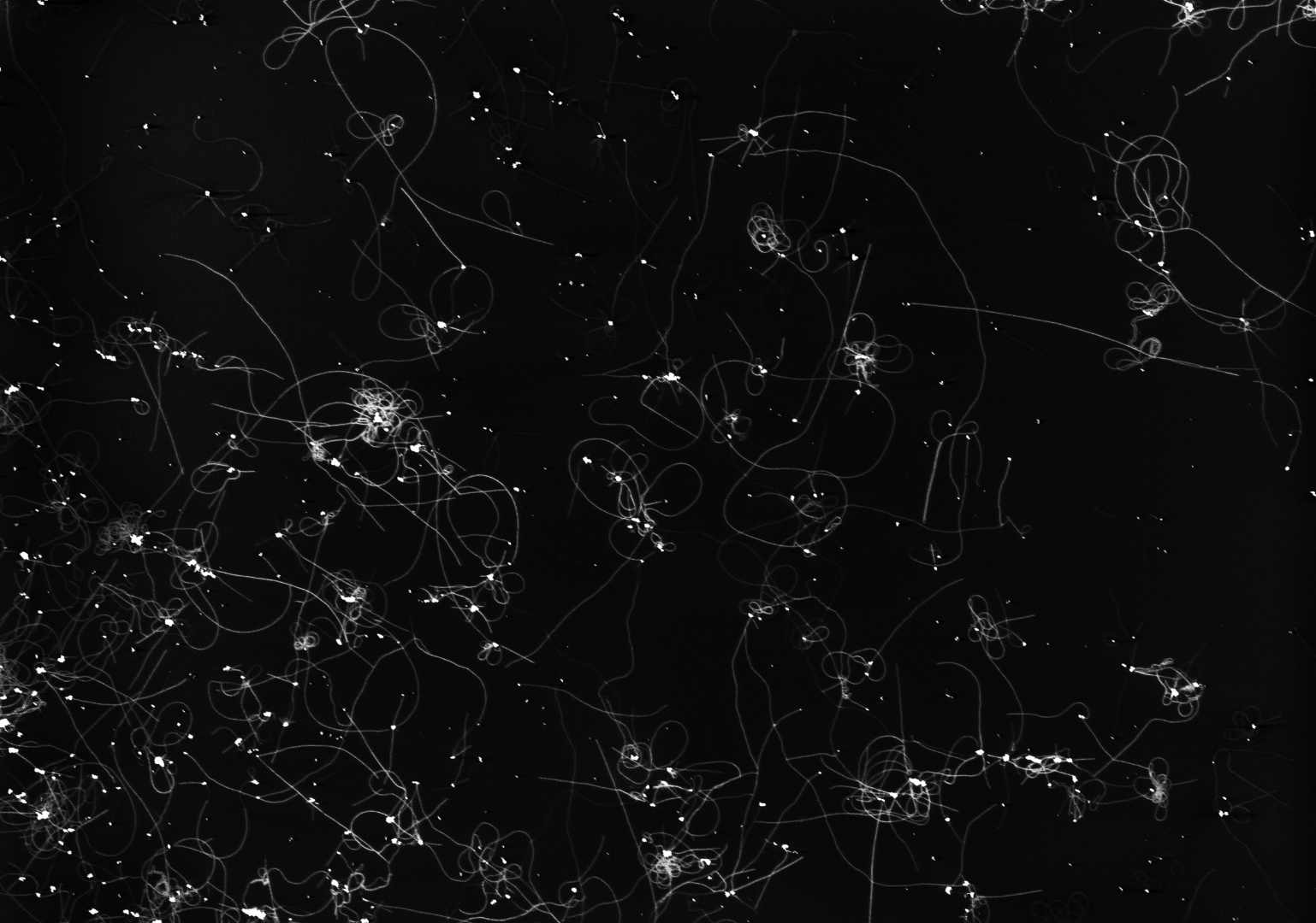
Dielectric breakdown in ebeam resist
When electron beam lithography is done on insulating substrates not coated with a conducting film, exposure of the resist during dielectric breakdown can result in a beautiful failure! Image courtesy of William Shattuck and Peter Gea.
Exfoliated MnPSe3
Thin film interference produces all the colors of the rainbow for this extremely cleavable layered antiferromagnet.
Machined aluminum at 200x magnification
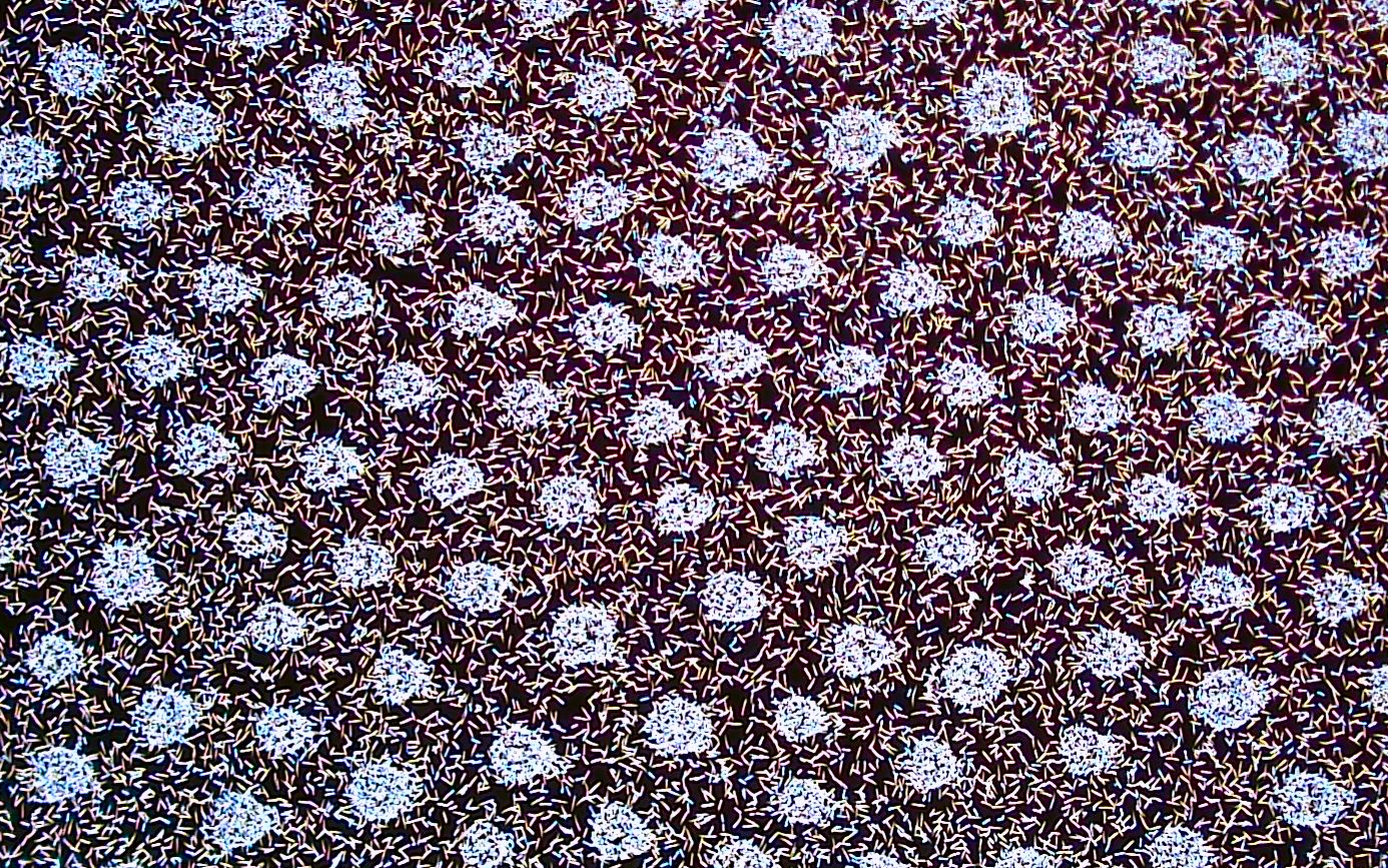
Hexagonal lattice of Te nanowire clusters
Self-assembled lattice of nanowire clusters organized during physical vapor deposition growth of tellurium. Image courtesy of Rabindra Basnet and Krishna Pandey.
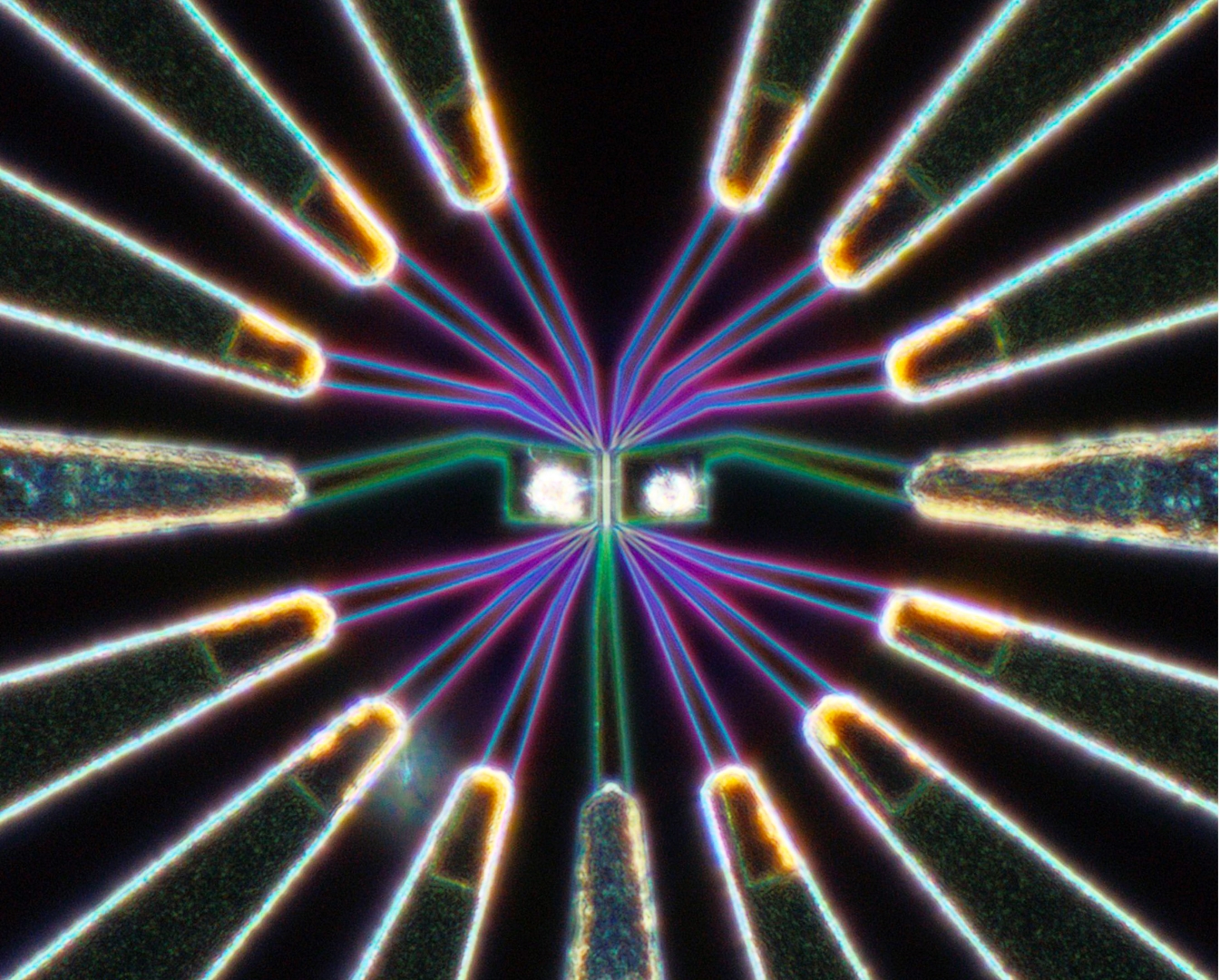
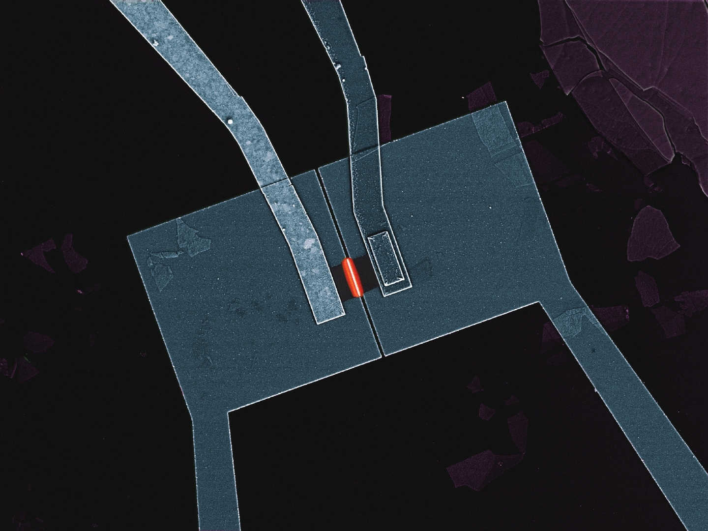
Carbon nanotube double quantum dot
Dark-field optical microscope image of a carbon nanotube grown over pre-patterned contacts and gate electrodes. With Charles Marcus group, Harvard University.
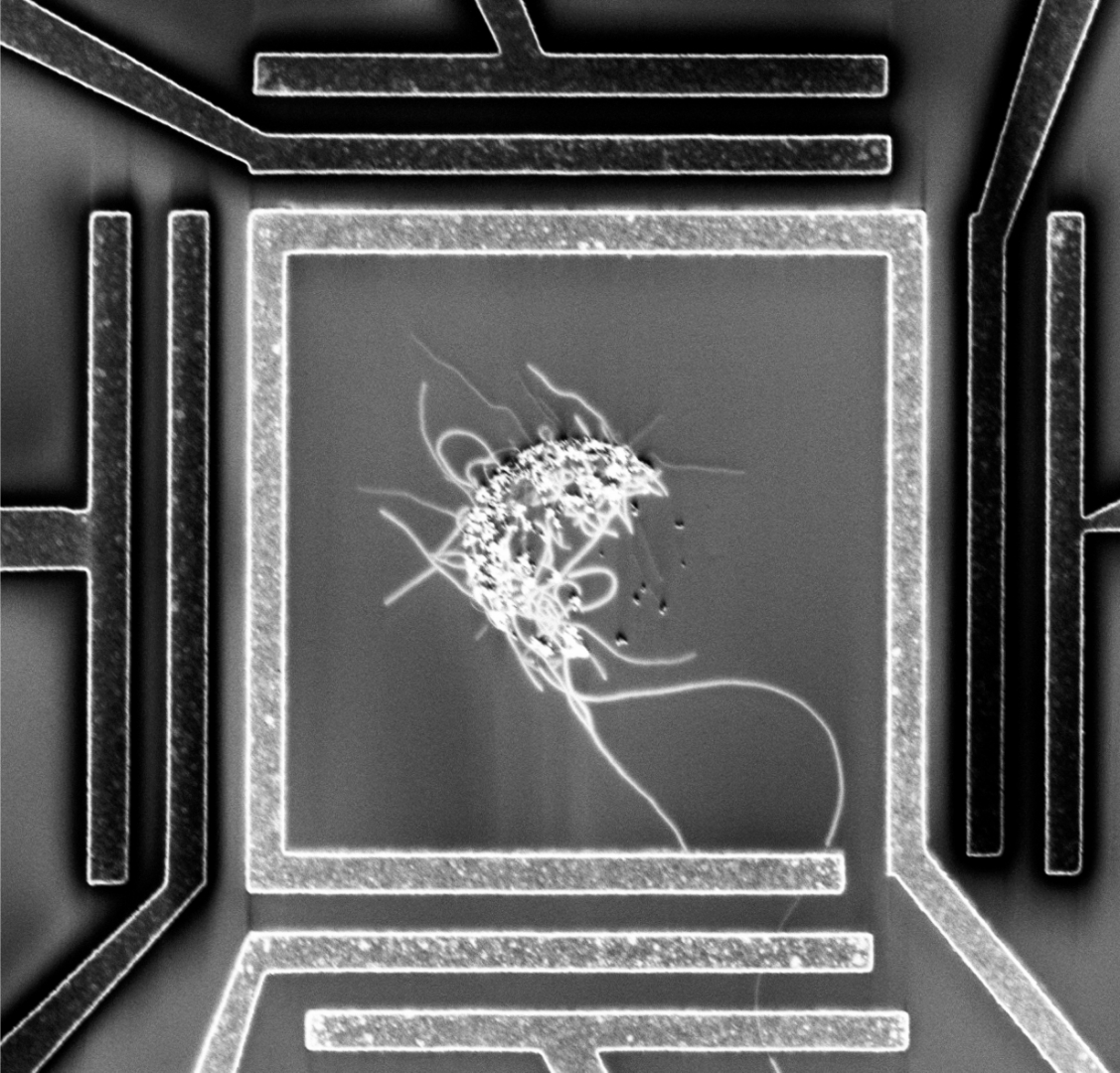
Carbon nanotube growth
SEM image of CVD-grown carbon nanotubes, contrast inverted. With Charles Marcus group, Harvard University.
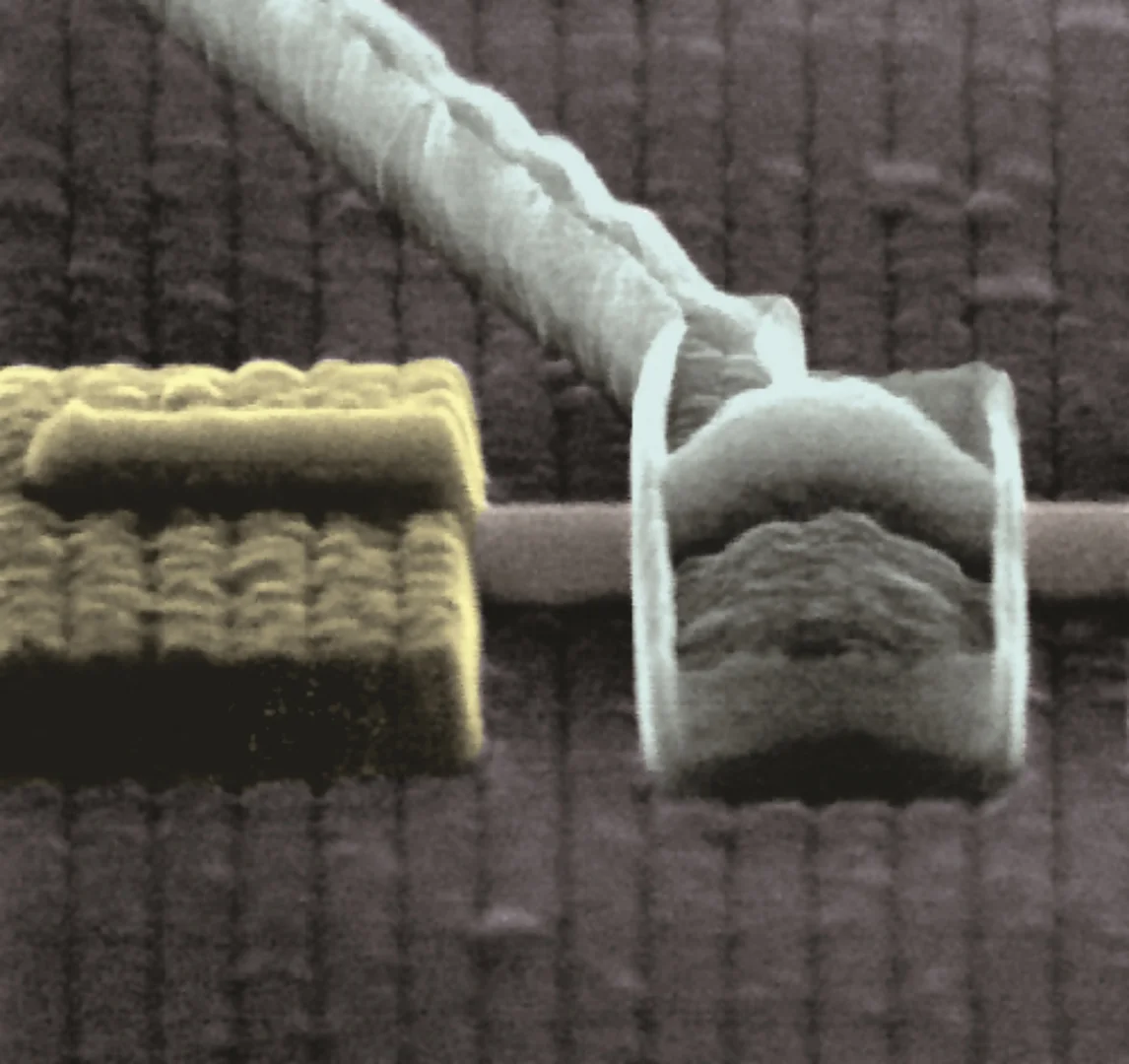
Carbon nanotube quantum dot
SEM image of a carbon nanotube draped over pre-patterned contact metal. The metal is lighter where contacted by the nanotube because those lines are shorted together and have a longer RC charging time in the SEM. With Charles Marcus group, Harvard University.
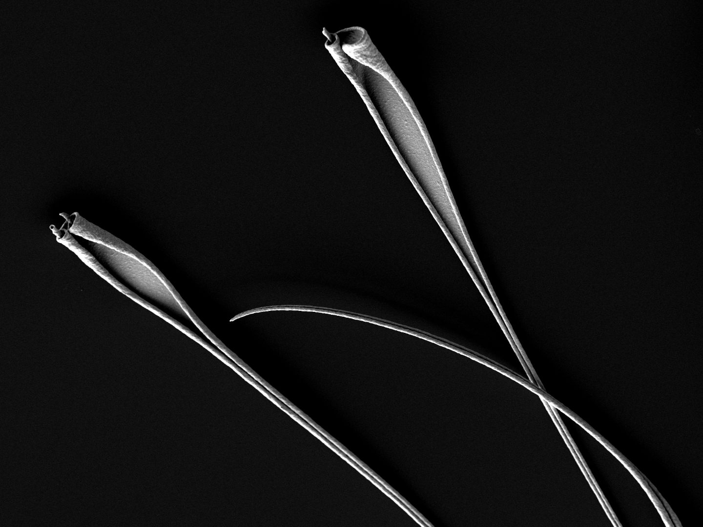
Curled platinum-gold metal bilayer
Bond pads for a device curled up during carbon nanotube growth at 900 degrees C, resulting in this attractive fabrication mistake. With Charles Marcus group, Harvard University.
InSb superconducting nanowire device
An InSb nanowire is contacted on the left by gold and on the right by the superconductor NbTiN for tunneling measurements. With Charles Marcus group, Harvard University.
Atomically thin WSe2 LED
Scanning electron micrograph of a three-atom thick WSe2 LED, with an artificial rendering of the light emission. With Pablo Jarillo-Herrero group, MIT; image credit Hugh Churchill and Felice Frankel.
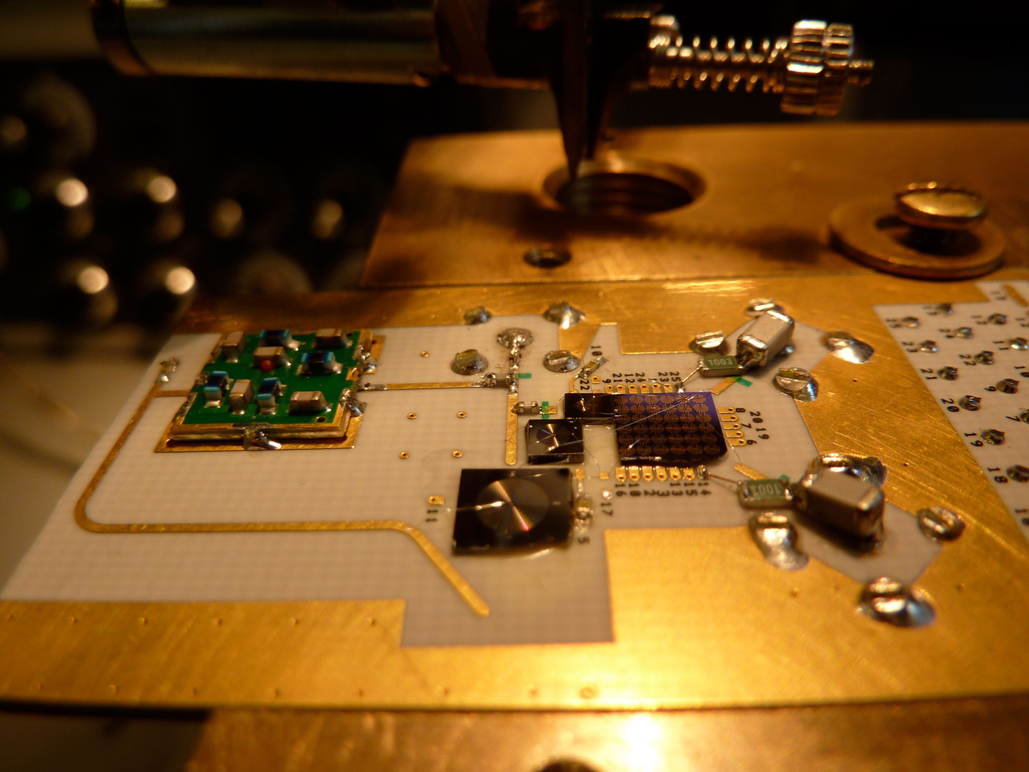
Reflectometry PCB
Custom PCB for radio frequency reflectometry measurements of carbon nanotube quantum dots. With Charles Marcus group, Harvard University.